Our Scientific Focus
We are concerned with the fundamental question "how we can tailor the optoelectronic properties of semiconductors, notably the nature of their photoexcitations, by employing external stimuli such as adjusting the local environment or using local fields?”
Semiconductor materials are without doubt the cornerstone of modern electronic and photonic technology, and central to sustainable economic growth. This applies to both organic and inorganic semiconductors. In general, the nature of photoexcitations is very different in both types of materials. For inorganic bulk semiconductors, strong covalent bonds allow for delocalized excitations and a high dielectric screening between charges, whereas in organic semiconductors the weak van-de-Waals-Coupling between adjacent chromophores implies localized excitations with strong Coulomb attraction between electron and holes. By now, the computer chip industry has pushed the structuring of bulk inorganic semiconductors to smaller and smaller lengths scales so that spatial confinement implies localized excitations. Conversely, the advent of supramolecular architectures and morphological control of semiconducting chromophores allows for delocalized photo excitations. As a result, the two communities frequently address similar questions, yet without benefitting from each other’s insights and worse, often with significant miscommunication. This is a scientific issue this graduate school wishes to address both in its research and in its qualification programme.

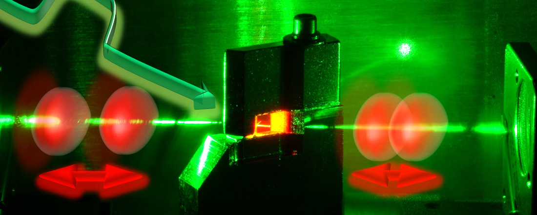
A focus in both communities is how we can modify the functionality of a semiconductor. In the last decade, organic and inorganic semiconductors have been used for optoelectronic applications that are made of nanoscale building blocks such as organic molecules, nanoparticles or colloids. In these cases, the functionality of an optoelectronic nanomaterial has traditionally been defined and fixed through its building blocks. To allow for different functions, such as light emission, sensing, signalling, or energy harvesting, chemically different building blocks have needed to be used. Here, we want to use a radically different, i.e. biomimetic approach. Nature accomplishes distinct functionalities in optically active systems by adjusting the local environment to realize specific functionalities. Classic examples are charge and energy transfer processes in light-harvesting proteins, where the embedding matrix is adapted to modify the transfer dynamics. We want to apply a similar approach to our organic and inorganic man-made photoactive systems. Our aim is to use external stimuli to define the functionality of the semiconductor, without changing its chemical composition. As external stimuli, we shall use both light and matter. The light part encompasses quasi-static and optical electromagnetic fields that will be shaped in space and time. The matter part is controlled in its internal structural order and its dimensionality.
Our research programme has thus two unique major innovative elements:
- We use a biomimetic approach of external control to alter the functionality of a semiconductor material.
- We apply this to a range of organic and inorganic nanostructured materials with a view to identifying common concepts and approaches and developing a common language for these usually disjoint communities.
The principal investigators and the research students will benefit from the insights they obtain through comparisons of the scientific approaches used and they will also benefit from the closer collaboration with scientists from both fields. We believe this will lead to accelerated rates and advances in the design of new materials and novel device concepts, and it is likely to lead to a more unified understanding of the physical principles behind excitons in nanostructured matter.
We are inspired by grand challenges that we will approach with the framework of external control of the interaction between excitations and light.
- How can we employ external stimuli to modify the energy landscape of a semiconductor so that for example an energetic funnel is written from outside into an otherwise homogeneous material? Such a funnel would guide the excitation energy to a well-defined position. This is addressed in projects 05 and 02.
- How can we realize coherent coupling for optical excitations in a macroscopic space, defined from outside, ideally with control over the wave function? Such a construct would act as quantum simulator for, e.g. organic semiconductors. These questions relate to projects 01, 03 and 06.
- How can we control the point in space at which coherent transport of excitation decays into incoherent localisation of the excitation? Is it also possible to reverse this process? Coherent transport is fast, but recombination needs localisation of the excitation. Projects 01, 03, 04 and 07 consider this issue.